


IBM has unveiled what it describes as the world's first sub-1nm chip technology, marking another ambitious step in the race to make processors faster, denser, and far more energy efficient. The company's latest research centres on a 7-angstrom, or 0.7nm, process node powered by a new transistor design called nanostack. IBM says the technology can pack close to 100 billion transistors into an area smaller than a human fingernail, roughly doubling the transistor density of its earlier 2nm design.
That sounds like a huge leap, and it is. But there is an important distinction: this is a research breakthrough, not a chip that is about to appear in the next generation of laptops, smartphones, or gaming PCs.
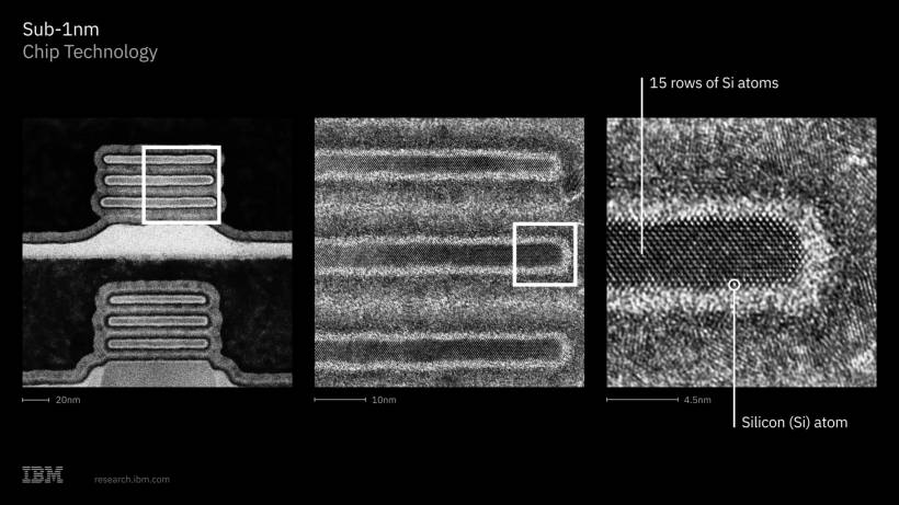
A New Milestone Beyond 2nm
For years, the semiconductor industry has continued to shrink transistors so that more of them can fit inside the same physical space. More transistors generally mean more processing power, better efficiency, and improved performance for everything from AI servers to mobile devices.
IBM's 7-angstrom design goes beyond its earlier 2nm nanosheet technology, which the company introduced as a major milestone in 2021.
The new architecture is intended to push chip design into what IBM calls the "angstrom era", where advances are no longer driven only by making components smaller on a flat surface. Instead, the industry is beginning to stack and arrange transistor structures in more sophisticated three-dimensional layouts.
IBM claims its 7A technology could offer:
These are projected gains based on IBM's research and experimental validation, rather than guarantees for a finished consumer processor.
What Is IBM's Nanostack Architecture?
The key development is IBM's new nanostack transistor architecture.
Modern leading-edge chips already use extremely small nanosheet transistors. IBM's approach takes this further by vertically stacking and staggering transistor layers, allowing the company to make more effective use of the third dimension.
Instead of expanding only sideways across a chip wafer, IBM is attempting to build upward.
This gives the design several potential advantages:
IBM says the design was tested through advanced wafer bonding, multi-channel engineering, and functioning CMOS inverter demonstrations. In simple terms, the company is not presenting only a concept drawing. It says the architecture has been physically demonstrated and can perform basic electronic switching operations.
Why 7 Angstrom Does Not Mean Everything Is Literally 0.7nm Wide
Chip node names can be confusing.
A label such as 7A, 2nm, 3nm, or Intel 18A does not always describe one exact physical measurement in the same way it did decades ago. Modern node names are generally used to describe a new generation of manufacturing technology, transistor density, performance characteristics, and design capability.
So, IBM's 7-angstrom announcement should not be read as meaning every part of the chip is physically 0.7nm wide.
What matters more is the claimed improvement in density and efficiency. IBM is saying it has found a way to create a much denser transistor structure than its existing 2nm platform while keeping the design functional.
Why This Matters for AI and High-Performance Computing
The timing of this research is closely tied to the rapid growth of AI.
Large AI models require enormous amounts of computing power. Training and operating them consumes vast quantities of electricity, while data centres are under growing pressure to increase performance without increasing power consumption at the same rate.
A more efficient transistor architecture could eventually help with:
IBM estimates that a future AI accelerator using 7A technology could potentially deliver around six times the performance of current leading accelerators, although this remains a forward-looking research estimate rather than a commercial benchmark.
Do Not Expect a 0.7nm Consumer CPU Soon
As exciting as the headline is, this technology is still some distance away from mass production.
IBM has not announced a commercial launch date for a 7A processor. The company itself has indicated that large-scale adoption of 2nm technology is still expected closer to the end of the decade, with 1.4nm and 1nm generations likely to follow after that.
That shows just how early this 7A work is.
Even 2nm manufacturing remains difficult and expensive. Japan's Rapidus, which works with IBM on advanced semiconductor technology, is targeting 2nm mass production by 2027. Before the industry can move confidently toward sub-1nm nodes, manufacturers will need to solve major challenges around yields, equipment, materials, cost, heat, and reliable large-scale production.
In other words, IBM's new design may influence the future of semiconductors, but consumers should not expect a "0.7nm laptop chip" to arrive anytime soon.
More Likely for Enterprise and AI Hardware First
When this class of technology eventually becomes practical, it will likely appear first in high-value enterprise systems.
That could include AI accelerators, data-centre processors, supercomputers, scientific computing systems, and specialised infrastructure where performance-per-watt matters more than retail affordability.
IBM's customer base is heavily focused on enterprise technology, research, hybrid cloud, and advanced computing. That makes it more likely that any early real-world use of nanostack-style technology would be found in large-scale systems before it reaches everyday consumer products.
Over time, successful chip architectures usually filter down. Innovations that begin in enterprise or server hardware can later influence processors used in desktops, laptops, phones, vehicles, and other connected devices.
Final Thoughts
IBM's 7-angstrom nanostack announcement is a major research milestone because it shows that chip scaling still has room to move forward, even as traditional transistor shrinking becomes increasingly difficult.
The real breakthrough is not simply the "sub-1nm" label. It is IBM's attempt to move chip design into a more advanced 3D era, where transistors are stacked, materials are tuned more precisely, and efficiency gains come from smarter architecture rather than only smaller dimensions.
There is still a long road between a laboratory breakthrough and a mass-produced processor. But if IBM's nanostack approach proves scalable, it could help shape the chips that power the next generation of AI, data centres, and high-performance computing.


Comments