

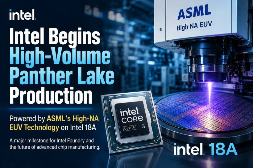
Intel has reached an important manufacturing milestone by moving selected Panther Lake Core Ultra 3 Series processors into high-volume production using ASML's advanced High Numerical Aperture extreme ultraviolet lithography technology.
The achievement is significant not only for Panther Lake, but also for Intel Foundry's broader effort to rebuild its position as a leading semiconductor manufacturer. Successfully introducing High-NA EUV into volume production demonstrates that Intel's Oregon fabrication facility can use one of the industry's most advanced chipmaking systems on its new Intel 18A process node.
Panther Lake Becomes an Important Test for Intel 18A
Panther Lake is the first major processor family built around Intel's 18A manufacturing process. As a result, its success will be closely watched by customers, investors and competitors.
Intel 18A represents a major step in the company's process roadmap. The node is expected to support smaller and more densely packed transistor designs while introducing technologies intended to improve performance and power efficiency.
Moving Panther Lake into high-volume manufacturing indicates that Intel is progressing beyond laboratory testing and early development wafers. The company is now demonstrating that selected parts of the manufacturing process can operate repeatedly at the scale required for commercial processor production.
That distinction matters. Producing a few successful chips is very different from manufacturing large quantities consistently while maintaining acceptable yields, performance and reliability.
What High-NA EUV Actually Does
Modern processors contain billions of extremely small transistors connected through increasingly complex layers of circuitry. Creating these structures requires advanced lithography machines that project intricate patterns onto silicon wafers.
Current EUV systems already use light with a wavelength of 13.5 nanometres to create smaller features than older deep ultraviolet lithography equipment can reliably produce.
High-NA EUV continues using the same 13.5nm wavelength, but upgrades the optical system's numerical aperture from 0.33 to 0.55.
Numerical aperture describes how effectively an optical system can collect and focus light. A higher numerical aperture allows the scanner to project finer and more detailed patterns onto the wafer.
In simpler terms, High-NA EUV works somewhat like using a more capable camera lens. It can resolve smaller details more accurately, helping manufacturers create denser chip designs that would be increasingly difficult to produce using existing equipment.
Why Smaller Circuit Patterns Are Becoming Harder to Manufacture
The semiconductor industry has continued shrinking transistor features to improve performance, efficiency and chip density. However, each new generation introduces greater manufacturing complexity.
As circuit patterns become smaller, the existing lithography equipment may no longer be able to print certain features clearly in a single exposure. Manufacturers must then divide one complicated pattern into several simpler ones and print them separately.
This technique is known as multi-patterning.
Although multi-patterning extends the usefulness of existing equipment, it adds more manufacturing steps. Each additional exposure requires extremely precise alignment with the previous layer.
Even tiny positioning errors can affect electrical performance, reduce manufacturing yields or cause a chip to fail completely.
High-NA EUV is designed to reduce this dependency by printing smaller and more detailed features directly.
Reducing the Need for Complex Multi-Patterning
One of the biggest advantages of High-NA EUV is its potential to simplify semiconductor manufacturing.
Without sufficient lithographic resolution, a chipmaker may need multiple masks and exposure cycles to create a single circuit layer. Every additional step consumes time, materials and production capacity.
It also increases the number of opportunities for defects or alignment problems to occur.
By using High-NA EUV for selected layers of the Intel 18A process, Intel may be able to reduce the amount of multi-patterning required. This can potentially provide:
The actual benefits will still depend on factors such as tool productivity, defect rates and wafer yields. High-NA EUV machines are highly advanced and expensive, so manufacturers must balance improved resolution against the cost of operating the equipment.
Why High-Volume Manufacturing Is the Real Milestone
Semiconductor companies frequently demonstrate new manufacturing technologies during research and development. The larger challenge is making those technologies dependable enough for continuous commercial production.
High-volume manufacturing requires the entire process to remain stable across many wafers and production cycles.
Intel must ensure that the High-NA EUV layers can be produced consistently while meeting strict requirements involving:
Qualifying the technology for volume production means Intel believes the process has reached a level where it can contribute to commercially manufactured products rather than remaining an experimental capability.
It also gives Intel valuable operational experience that could be used for future processor generations and external foundry customers.
A Major Step for Intel Foundry
The milestone is particularly important for Intel Foundry, the division responsible for producing chips for Intel itself and potentially for external customers.
Intel has invested heavily in expanding and modernising its fabrication capabilities. The company wants to compete more directly with major contract manufacturers by offering advanced production technologies to other chip designers.
To attract those customers, Intel Foundry must prove that its latest process nodes are not only technically impressive but also reliable, scalable and commercially practical.
Operating High-NA EUV on Intel 18A gives the foundry another capability it can present to potential customers. It suggests that Intel is gaining early experience with technology expected to become increasingly important as semiconductor designs continue shrinking.
Foundry customers will still examine manufacturing yields, pricing, design tools and delivery schedules before committing major products. Nevertheless, successful volume production is an important credibility milestone.
Keeping More Advanced Manufacturing In-House
The development may also help Intel retain greater control over the manufacturing of its most advanced processors.
When a company lacks the necessary internal production capability, it may need to outsource particular components or manufacturing stages to another foundry. Outsourcing can provide access to mature processes, but it also introduces greater dependency on external production capacity and scheduling.
By qualifying High-NA EUV layers internally at its Oregon facility, Intel can develop the process around its own processor architecture and manufacturing requirements.
Keeping more work in-house may provide tighter coordination between Intel's chip designers and manufacturing engineers. Problems discovered during production can be communicated directly between the teams responsible for the architecture, packaging and fabrication process.
It could also reduce reliance on external manufacturers for strategically important technologies, although Intel may continue using outside foundries where doing so makes technical or commercial sense.
Panther Lake Carries Broader Strategic Importance
Panther Lake is more than another annual processor refresh. It serves as an important demonstration of whether Intel can successfully combine its processor designs with its latest manufacturing platform.
Strong manufacturing execution could help Intel improve processor efficiency, product availability and competitiveness. Difficulties with yield or production scale, however, could affect costs and launch volumes.
The use of High-NA EUV does not automatically guarantee that Panther Lake will outperform competing processors. Final product performance will also depend on architecture, memory design, integrated graphics, packaging, software optimisation and power management.
Still, manufacturing technology provides the physical foundation on which all those features are built. A stable and efficient 18A process would give Intel more flexibility when designing future products.
High-NA EUV Is Likely to Shape Future Chip Generations
ASML's High-NA EUV systems are widely viewed as an important part of the semiconductor industry's next manufacturing phase.
Current EUV technology will continue to play a major role, but producing increasingly small and dense circuit patterns will eventually require more capable optical systems.
High-NA EUV could allow manufacturers to print critical layers with fewer exposures and better accuracy. This may become increasingly valuable for future processors, accelerators and other advanced semiconductor designs.
However, adoption will likely be gradual. Chipmakers may initially use High-NA EUV only on selected layers where its improved resolution provides the greatest benefit.
Existing EUV systems can continue handling less demanding layers, helping manufacturers control costs while they gain experience with the newer equipment.
Intel's Panther Lake production appears to follow this practical approach by using High-NA EUV for selected manufacturing layers rather than replacing the entire lithography process at once.
Final Thoughts
Intel's move into high-volume Panther Lake manufacturing using ASML's High-NA EUV technology represents an important achievement for both the company's processor roadmap and its foundry ambitions.
The milestone confirms that Intel's Oregon facility has qualified High-NA EUV layers for its advanced 18A process, moving the technology beyond experimentation and into commercial production.
By enabling finer circuit patterns, High-NA EUV could reduce the need for complicated multi-patterning, improve manufacturing accuracy and help Intel maintain greater control over advanced chip production.
The real test will be whether Intel can sustain strong yields, reliable output and competitive performance as Panther Lake reaches the market. Even so, successfully bringing High-NA EUV into volume manufacturing gives Intel Foundry an important early advantage in the next stage of semiconductor production.











Comments 0